Siemens unveils tools for advanced 2.5D & 3D IC design
Thu, 26th Jun 2025
Siemens Digital Industries Software has announced the addition of two new products to its Electronic Design Automation (EDA) portfolio, aimed at addressing the challenges presented by 2.5D and 3D Integrated Circuit (IC) design and manufacturing.
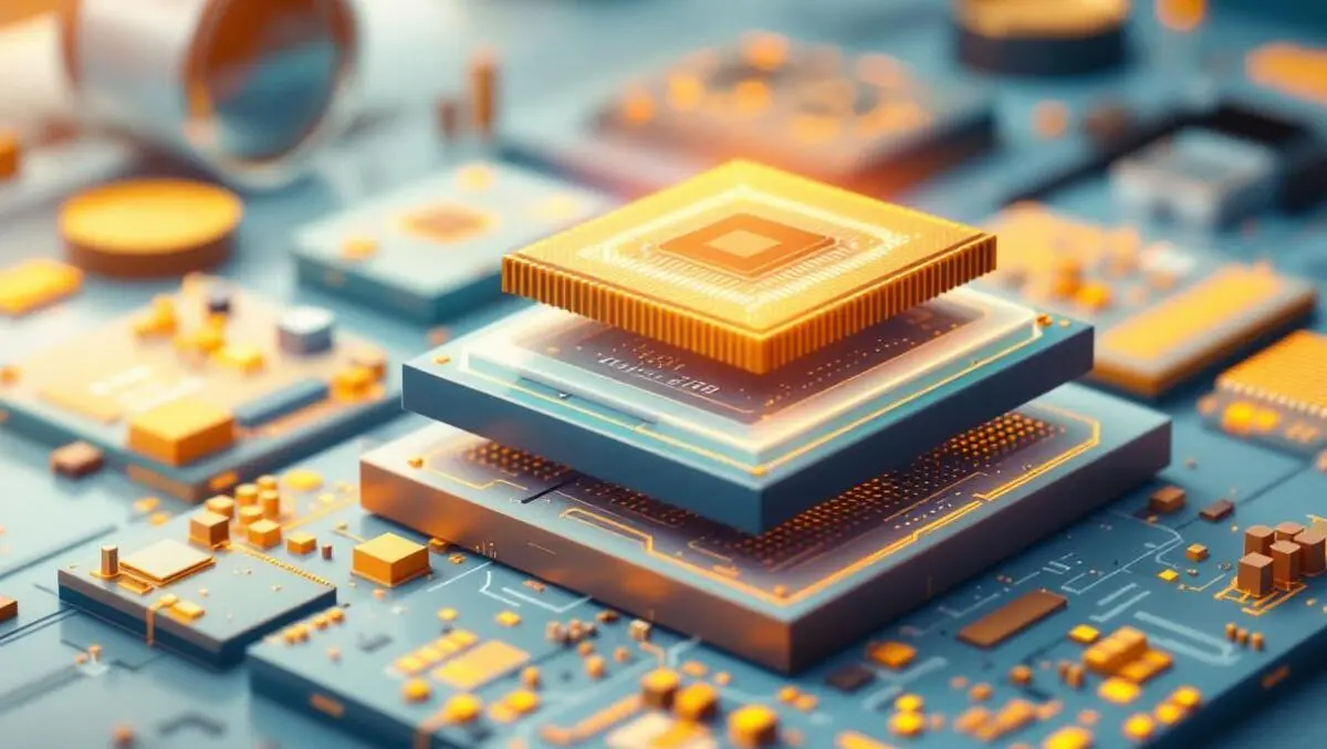
The new Innovator3D IC suite is designed to help integrated circuit designers manage the increasing complexity of heterogeneously integrated 2.5D and 3D IC architectures. Alongside this suite, Siemens launched Calibre 3DStress, a software tool intended to provide early and accurate thermo-mechanical analysis, including the effects of stress at the transistor level during chip and package integration.
Addressing complexity in IC design
According to the company, the electronics industry is now incorporating thinner dies and higher package processing temperatures into 2.5D and 3D IC designs. This has resulted in situations where ICs that pass validation at the die level may encounter issues with specification compliance once assembled and reflowed in final packaging. These issues can impact both the performance and reliability of devices.
The Innovator3D IC solution suite is intended to streamline several design and management tasks. It incorporates functions for planning, heterogeneous integration, substrate and interposer implementation, interface protocol analysis compliance, and management of design data and intellectual property (IP).
Built with an artificial intelligence-driven user experience, the suite leverages extensive multithreading and multicore processing to tackle designs with over five million pins. The suite includes: the Innovator3D IC Integrator for unified design planning and predictive analysis using a digital twin; the Innovator3D IC Layout, which supports package interposer and substrate implementation; the Innovator3D IC Protocol Analyzer for chiplet-to-chiplet and die-to-die interface compliance; and the Innovator3D IC Data Management element for managing work-in-progress designs and data IP.
Early detection of design risks
Calibre 3DStress expands Siemens' multiphysics solution introduced with Calibre 3DThermal in 2024. Calibre 3DStress is tailored for transistor-level analysis, verification and debugging of mechanical stresses - including warpage - within 3D IC packages. The software lets engineers predict the effects of chip-package interaction on overall design function earlier in the process, aiming to prevent potential failures and optimise for durability and performance.
The tool is distinguished by its ability to detect stress at the transistor rather than just the package level, providing visibility into electrical behaviour and potential risks earlier in the design process. This capability integrates industry-standard Calibre physical verification with an advanced mechanical solver for evaluating stresses in IC structures and materials.
Mike Ellow, Chief Executive Officer, Siemens EDA, Siemens Digital Industries Software said:
By delivering a stress-aware multiphysics analysis solution powered by Calibre 3DStress and driven by the Innovator3D IC solution suite, Siemens enables customers to overcome the complexities and risks associated with 3D IC designs. These capabilities are critical for our customers, allowing them to accelerate productivity and meet stringent design timelines by effectively eliminating the barriers of design complexity that traditionally impact design cycles.
Industry feedback
Several organisations in the semiconductor sector have evaluated Siemens' solutions for their own work in advanced platform integration.
Bryan Black, Chief Executive Officer of Chipletz, commented on the adoption of the new toolset in his company's design process.
In 2023, we adopted Siemens' technology to meet the complex design and integration challenges of our advanced platform solutions. The Innovator3D IC solution suite plays a critical role in enabling the high-performance solutions we deliver to AI and HPC datacenters.
Sandro Dalle Feste, APMS Central R&D Senior Director at STMicroelectronics, said of the Calibre 3DStress tool:
Siemens EDA's Calibre 3DStress tool can synthesize the complexity of components, materials and processes related to 3D IC architectures and can create accurate IP-level stress analysis. Using it, ST has been able to implement early design planning and sign-off flows, and accurately model potential electrical failures due to IP-level stress within a 3D IC package. The result is improved reliability and quality, together with a reduced time to market, which provide a win both for ST and our customers.
Continued development
Siemens states that the new tools will further extend its multiphysics software portfolio, forming a core part of its digital twin and semiconductor development workflows for advanced IC designs.